Korean company vies to roll out MEMS pins with annual sales target of W200 bil.
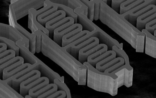
Point Engineering, a South Korean manufacturer of display and semiconductor parts, announced on May 24 that it would launch a ‘pin foundry’ business for semiconductor testing.The Asan-based corporation, some 90 kilometers south of Seoul, strives to produce high-end pins used for pre- and post-semiconductor process testing.Point Engineering noted that the new venture’s business structure is comparable to the semiconductor foundry process, where the fabrication plant and integrated circuit design operation are separated.Point Engineering rolls out customized test pins upon customer requests, as well as cranking out MEMS pins for semiconductor wafer-level testing and socket pins for semiconductor post-process packaging testing.Short for micro-electro-mechanical systems, MEMS constitute the technology of microscopic devices, especially those with moving parts.“The size of the semiconductor test pin market is expected to exceed 1 trillion won ($790 million) this year alone, but the market has high entry barriers from technical limitations of high integration and miniaturization of sockets and probe cards,” a Point Engineering official said.“However, we expect to secure an unrivaled position in the semiconductor test pin market by satisfying the four high requirements of high density, high frequency, high speed, and stability through our MEMS element technology, compared to the existing semiconductor test pin.”The company claimed that the most distinguishing difference of its test pins is the replacement of pre-existing photoresist mold with an anodic aluminum oxide (AAO) mold to produce a pin in a completely new method.Bold sales target
Point Engineering said that there are three major advantages of the AAO mold _ a high aspect ratio, the availability of fine patterning, and precision.“First of all, the existing photoresist method can only support the pin thickness by 20~30um, whereas a single AAO mold can support up to 100~110um. Through this feature of AAO, a width of 5um by 100um thickness mold can be formed,” the official said.“Secondly, it is the availability of fine patterning. Fine pattern gaps, as small as 4um, can be stably implemented to produce complex features of test pins. Precise technology can increase the number of beam strands of the pin body to increase the volume and surface area of the pin.”Finally, the official talked about the company product’s precision _ the upper and lower dimensional tolerances of its product made from the AAO mold, which consists of nano-sized pores, are only 0.5um.“We are trying to actively communicate with customers through active online sales activities and our website, unlike the existing companies that used closed sales methods, which restrict technology opening,” Point Engineering CEO Ahn Bum-mo said.“Although we are still in the early stages of the business, we are aggressively marketing to successfully enter and settle the market, and we will do our best to achieve initial sales of 50 billion won ($40 million) per year, which is 5 percent of the market size, to 200 billion won ($160 million), which is 20 percent, in the future.”이 기사를 공유합니다
Kevin Chung
(jumphigher55@aol.com)