Korean tech giant hosts Foundry Forum in US
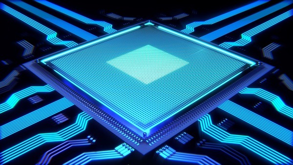
Samsung Electronics is ready for 3 nanometer (nm) technology, which will speed up innovations in advanced applications such as artificial intelligence and internet of things. One nanometer is a length that is one billionth of a meter, or about one 10,000th the diameter of a human hair.The Seoul-based company said May 15 that its 3 nm gate-all-around (GAA) process development is on track, noting that its process design kit version 0.1 for the technology has been released in April for customers.“Compared to 7nm technology, Samsung’s 3nm GAA process is designed to provide up to a 45 percent reduction in chip area with 50 percent lower power consumption or 35 percent higher performance,” a Samsung official said.“The GAA-based process node is expected to be widely adopted in next-generation applications, such as mobile, network, automotive, artificial intelligence, and internet of things.”The tech giant also announced its commitment to foundry innovation and service at the Samsung Foundry Forum 2019 USA, providing the silicon community with updates on latest technological advances.Samsung Electronics has put forth great efforts to diversify its revenue sources by reducing its dependence on memory chips whose demands are highly volatile. And one of its targets is the foundry market.“We stand at the verge of the fourth industrial revolution, a new era of high-performance computing and connectivity that will advance the daily lives of everyone on the planet,” Samsung President ES Jung said.“Samsung Electronics fully understands that achieving powerful and reliable silicon solutions requires not only the most advanced manufacturing and packaging processes as well as design solutions, but also collaborative foundry-customer relationships grounded on trust and shared vision.”He added that “This year’s Foundry Forum is filled with compelling evidence of our commitment to progress in all those areas, and we’re honored to host and converse with our industry’s best and brightest.”The Foundry Forum was held May 15 in Santa Clara, California, featuring senior Samsung executives and industry experts from across the world.이 기사를 공유합니다
Hillary Lee
(homin30@hanmail.net)