Korean company achieves feat for 1st time in world
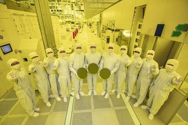
South Korea’s Samsung Electronics announced on June 30 that it had started rolling out chips using the 3-nanometer technology for the first time in the world.The company said that its gate-all-around (GAA) technology was adopted to improve power efficiency by reducing the supply voltage level while enhancing performance by raising drive current capability.Thus far, it has depended on the 4nm technology. Samsung is the world’s biggest manufacturer of memory chips, flat-panel displays, and smartphones.“Samsung has grown rapidly as we continue to demonstrate leadership in applying next-generation technologies to manufacturing, such as the foundry industry’s first High-K Metal Gate, FinFET, as well as EUV. We seek to continue this leadership with the world’s first 3nm process with the MBCFET,” Samsung President Choi Si-young said.“We will continue active innovation in competitive technology development and build processes that help expedite achieving maturity of the technology.”Samsung said that its first-generation 3nm process could reduce power consumption by up to 45 percent, improve performance by 23 percent and reduce the area by 16 percent compared to 5nm.Its second-generation 3nm process is expected to reduce power consumption by up to 50 percent, improve performance by 30 percent and reduce the area by 35 percent.“As technology nodes get smaller and chip performance needs grow greater, IC designers face challenges of handling tremendous amounts of data to verify complex products with more functions and tighter scaling,” a Samsung official said.“To meet such demands, Samsung strives to provide a more stable design environment to help reduce the time required for design, verification, and sign-off process, while also boosting product reliability.”Experts point out that the transition to the 3nm technologies is a huge change.“The 3nm process is a quantum level in the electro-engineering field. Samsung seemingly attempts to find a game-changer in the stiff competition with TSMC,” Prof. Kim Jung-ho at KAIST said.Samsung and Taiwan’s TSMC have staged a close rivalry to lead the global semiconductor business.이 기사를 공유합니다
Tim Kim
(voc200@gmail.com)